

ZMSH 12-inch (300mm) SiC single crystal wafers are high-purity, wide-bandgap semiconductors produced via Physical Vapor Transport (PVT) method. With excellent electrical, thermal, and mechanical properties, SiC wafers are ideal for high-power, high-voltage, and high-frequency applications, as well as GaN-based LED and laser diode substrates.

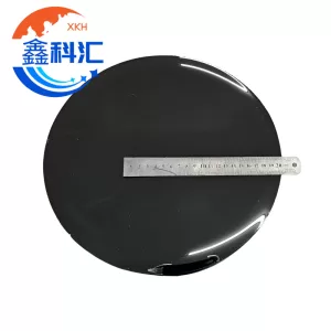
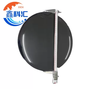
Our 12-inch wafers feature ultra-low basal plane dislocation (BPD) density, high thermal conductivity, and precise crystallographic orientation, ensuring superior device performance, reliability, and reproducibility.
| Property | 4H-SiC | 6H-SiC |
|---|---|---|
| Crystal Structure | Hexagonal | Hexagonal |
| Lattice Constant | a=3.08 Å, c=10.05 Å | a=3.08 Å, c=15.12 Å |
| Band Gap | 3.23 eV | 3.02 eV |
| Hardness (Mohs) | 9.2 | 9.2 |
| Thermal Conductivity (N-type, 0.02 Ω·cm) | a~4.2 W/cm·K, c~3.7 W/cm·K | a~4.6 W/cm·K, c~3.2 W/cm·K |
| Thermal Expansion Coefficient | 4–5×10⁻⁶/K | 4–5×10⁻⁶/K |
| Dielectric Constant | ~9.66 | ~9.66 |
| Resistividad | 0.015–0.028 Ω·cm (N-type) | >1×10⁵ Ω·cm (Semi-insulating) |
| Orientation | <0001>, 4° off-axis | <0001>, 4° off-axis |
| Pulido | Single-side or double-side | Single-side or double-side |
| Surface Roughness | Ra ≤ 5Å | Ra ≤ 5Å |
| TTV | ≤15 µm | ≤15 µm |
| Bow/Warp | ≤80 µm | ≤80 µm |
| Thickness | 0.35–1.0 mm (customizable) | 0.35–1.0 mm (customizable) |
| Monocrystal Zone | ≥290 mm | ≥290 mm |
| EPD (Etch Pit Density) | ≤1/cm² | ≤1/cm² |
| Chiping | ≤2 mm | ≤2 mm |
1. Power Electronics:
SiC MOSFETs, PiN diodes, Schottky diodes (SBD), JBS diodes, IGBTs, and SiC BJTs.
High-efficiency power modules with smaller size, lighter weight, and reduced energy loss compared to silicon.
Supports devices operating at high voltages (3kV–12kV) and high temperatures.
2. Optoelectronic Devices:
Substrate for GaN-based LEDs and laser diodes.
Excellent lattice match and thermal compatibility with GaN layers improves light extraction efficiency y heat dissipation.
Enables vertical device structures without current diffusion layer.
3. Research & Advanced Devices:
Suitable for experimental research in BPD reduction, high-voltage devices, and next-generation SiC electronics.
Used in high-frequency and high-temperature electronic devices.
Low BPD Density:
Optimized PVT growth, seed bonding, and graphite crucible selection reduce basal plane dislocations below 1000 cm⁻², improving reliability of high-power and high-voltage devices.
Excellent Thermal & Electrical Performance:
High thermal conductivity ensures effective heat dissipation.
Wide bandgap and high electron mobility minimize energy loss under high voltage and high temperature.
Large 12-Inch Diameter:
Enables mass production of power devices and LED substrates.
Customizable thickness, resistivity, and orientation for specific applications.
High-Quality Surface Finish:
Single-side or double-side polished wafers with ultra-low roughness (Ra ≤ 5Å) ensure uniform epitaxial growth.
Cleanroom Packaging:
Each wafer packaged individually in a 100-grade clean environment to prevent contamination.
Q1: What is the typical BPD density of ZMSH 12-inch SiC wafers?
A1: Basal plane dislocation density is controlled below 1000 cm⁻² through optimized growth, cooling, and seed bonding processes, ensuring superior device reliability.
Q2: Can the wafer thickness, orientation, or resistivity be customized?
A2: Yes. Thickness (0.35–1.0 mm), off-axis orientation (<0001> 4° or custom), and resistivity (N-type 0.015–0.028 Ω·cm or semi-insulating >1×10⁵ Ω·cm) can all be customized.
Q3: How does SiC substrate benefit GaN-based LED applications?
A3: SiC provides lattice and thermal compatibility with GaN, allows vertical device structure, improves light extraction efficiency, and enhances thermal management, enabling longer device lifespan.
ZMSH is dedicated to providing high-performance 12-inch SiC wafers with ultra-low dislocation density and reproducible quality. Our wafers are ideal for power electronics, optoelectronics, and next-generation semiconductor research, with customizable specifications to meet industrial and research needs.