

ZMSH 12-inch (300mm) SiC single crystal wafers are high-purity, wide-bandgap semiconductors produced via Physical Vapor Transport (PVT) method. With excellent electrical, thermal, and mechanical properties, SiC wafers are ideal for high-power, high-voltage, and high-frequency applications, as well as GaN-based LED and laser diode substrates.

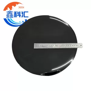
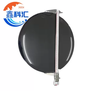
Our 12-inch wafers feature ultra-low basal plane dislocation (BPD) density, high thermal conductivity, and precise crystallographic orientation, ensuring superior device performance, reliability, and reproducibility.
| Property | 4H-SiC | 6H-SiC |
|---|---|---|
| Crystal Structure | Hexagonal | Hexagonal |
| Lattice Constant | a=3.08 Å, c=10.05 Å | a=3.08 Å, c=15.12 Å |
| Band Gap | 3.23 eV | 3.02 eV |
| Hardness (Mohs) | 9.2 | 9.2 |
| Thermal Conductivity (N-type, 0.02 Ω·cm) | a~4.2 W/cm·K, c~3.7 W/cm·K | a~4.6 W/cm·K, c~3.2 W/cm·K |
| Wärmeausdehnungskoeffizient | 4–5×10⁻⁶/K | 4–5×10⁻⁶/K |
| Dielectric Constant | ~9.66 | ~9.66 |
| Widerstandsfähigkeit | 0.015–0.028 Ω·cm (N-type) | >1×10⁵ Ω·cm (Semi-insulating) |
| Orientierung | <0001>, 4° off-axis | <0001>, 4° off-axis |
| Polieren | Single-side or double-side | Single-side or double-side |
| Surface Roughness | Ra ≤ 5Å | Ra ≤ 5Å |
| TTV | ≤15 µm | ≤15 µm |
| Bow/Warp | ≤80 µm | ≤80 µm |
| Dicke | 0.35–1.0 mm (customizable) | 0.35–1.0 mm (customizable) |
| Monocrystal Zone | ≥290 mm | ≥290 mm |
| EPD (Etch Pit Density) | ≤1/cm² | ≤1/cm² |
| Chiping | ≤2 mm | ≤2 mm |
1. die Leistungselektronik.
SiC MOSFETs, PiN diodes, Schottky diodes (SBD), JBS diodes, IGBTs, and SiC BJTs.
High-efficiency power modules with smaller size, lighter weight, and reduced energy loss compared to silicon.
Supports devices operating at high voltages (3kV–12kV) and high temperatures.
2. Optoelectronic Devices:
Substrate for GaN-based LEDs and laser diodes.
Excellent lattice match and thermal compatibility with GaN layers improves light extraction efficiency and heat dissipation.
Enables vertical device structures without current diffusion layer.
3. Research & Advanced Devices:
Suitable for experimental research in BPD reduction, high-voltage devices, and next-generation SiC electronics.
Used in high-frequency and high-temperature electronic devices.
Low BPD Density:
Optimized PVT growth, seed bonding, and graphite crucible selection reduce basal plane dislocations below 1000 cm⁻², improving reliability of high-power and high-voltage devices.
Excellent Thermal & Electrical Performance:
High thermal conductivity ensures effective heat dissipation.
Wide bandgap and high electron mobility minimize energy loss under high voltage and high temperature.
Large 12-Inch Diameter:
Enables mass production of power devices and LED substrates.
Customizable thickness, resistivity, and orientation for specific applications.
High-Quality Surface Finish:
Single-side or double-side polished wafers with ultra-low roughness (Ra ≤ 5Å) ensure uniform epitaxial growth.
Cleanroom Packaging:
Each wafer packaged individually in a 100-grade clean environment to prevent contamination.
Q1: What is the typical BPD density of ZMSH 12-inch SiC wafers?
A1: Basal plane dislocation density is controlled below 1000 cm⁻² through optimized growth, cooling, and seed bonding processes, ensuring superior device reliability.
Q2: Can the wafer thickness, orientation, or resistivity be customized?
A2: Yes. Thickness (0.35–1.0 mm), off-axis orientation (<0001> 4° or custom), and resistivity (N-type 0.015–0.028 Ω·cm or semi-insulating >1×10⁵ Ω·cm) can all be customized.
Q3: How does SiC substrate benefit GaN-based LED applications?
A3: SiC provides lattice and thermal compatibility with GaN, allows vertical device structure, improves light extraction efficiency, and enhances thermal management, enabling longer device lifespan.
ZMSH is dedicated to providing high-performance 12-inch SiC wafers with ultra-low dislocation density and reproducible quality. Our wafers are ideal for power electronics, optoelectronics, and next-generation semiconductor research, with customizable specifications to meet industrial and research needs.