Innehållsförteckning
Si wafers, commonly referred to as Silicon wafers, represent a cornerstone of modern technological innovation, serving as the essential foundation for the fabrication of integrated circuits (ICs) and various semiconductor devices. These thin slices of single-crystal silicon are indispensable components that underpin the development of intricate electronic systems driving advancements across numerous industries. This expanded abstract offers a detailed exploration of Si wafers, encompassing their intricate manufacturing techniques, nuanced physical attributes, diverse applications, and the dynamic evolution of semiconductor technology.
Manufacturing Techniques:
The production of silicon wafers involves a sophisticated series of manufacturing techniques designed to create substrates of unparalleled quality. This process typically initiates with the growth of a single-crystal silicon ingot, achieved through methodologies like the Czochralski process or the Float Zone technique. The resulting ingot is meticulously sliced into thin wafers using advanced cutting tools, with utmost precision to minimize material wastage. Subsequent steps entail surface treatments to eliminate impurities and defects, followed by polishing and cleaning procedures to achieve the desired surface smoothness and cleanliness crucial for semiconductor fabrication.
Physical Characteristics:
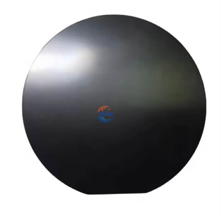
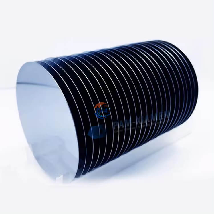
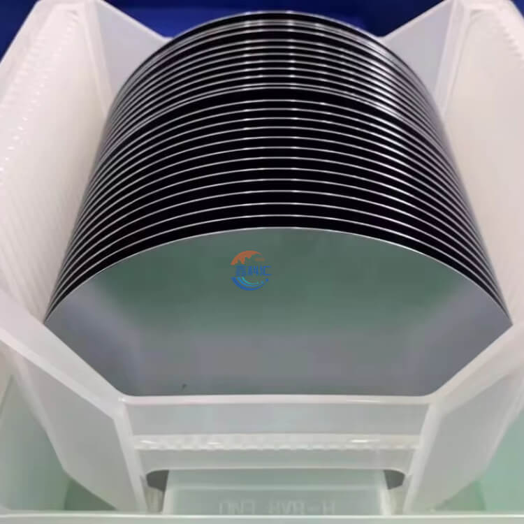
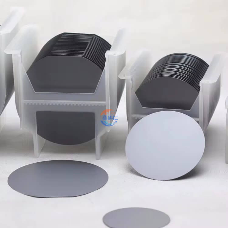
Silicon wafers possess a plethora of physical characteristics that render them ideally suited for semiconductor applications. Primarily comprising single-crystal structures, these wafers exhibit uniform lattice orientations, ensuring consistent electrical performance across their surfaces. Available in various diameters and thicknesses, ranging from a few inches to over a foot in diameter and from tens to hundreds of micrometers in thickness, Si wafers offer versatility to accommodate diverse device requirements. The meticulously engineered wafer surfaces present an immaculate canvas conducive to the precise patterning of electronic components during subsequent manufacturing phases.
Wide-Ranging Applications:
The utility of Si wafers extends across a broad spectrum of industries, with the semiconductor sector standing as the primary beneficiary. These wafers serve as the substrate material for the production of ICs, microprocessors, memory modules, and an array of electronic components integral to modern computing and communication devices. Beyond the realm of microelectronics, Si wafer play a pivotal role in photovoltaic cell manufacturing for solar energy applications. Additionally, they find application in the creation of sensors, MEMS devices, and various microsystems essential to sectors ranging from automotive to medical electronics.
In conclusion, Si wafer stand as indispensable enablers of technological progress, serving as the bedrock upon which the modern semiconductor industry thrives. Their intricate manufacturing processes, unique physical characteristics, diverse applications, and pivotal role in advancing semiconductor technology underscore their significance in shaping the trajectory of innovation. As the semiconductor landscape continues to evolve, silicon wafers are poised to remain at the forefront of technological advancement, driving continued innovation and ushering in new possibilities across various industries.
| Produkt. | Kiselskiva (Si) |
| Betyg. | IC förstklassig kvalitet |
| Renhet. | >99,9999999999999% (11N) |
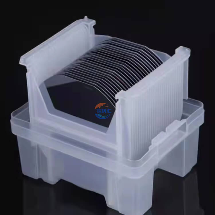
| Dimension. | Standardmått.- 1” × 0,5 mm - 2” × 0,28 / 0,4 / 0,5 mm - 3” × 0,38 mm - 4 ” × 0,525 mm- 5” × 0,6 mm- 6” × 0,625 mm- 8” × 0,725 mm Andra diametrar och tjocklekar tillgängliga- Vi tillhandahåller småskaliga icke-standardiserade wafers för forsknings- och teständamål. |
| Orientering. | / / / off-axis / övriga |
| Ledande typ. | - O-dopad (även kallad intrinsic, native) typ- N-typ: fosfor (P)-dopad- P-typ: bor (B)-dopad |
| Resistivitet. | Standardresistivitet för odopade wafers.- 3000 - 6000 Ω-cm Standardresistivitet för wafers av n-/ p-typ.- 0,001 - 0,009 Ω-cm- 1 - 10 Ω-cm- 10 - 20 Ω-cm- 90 - 100 Ω-cm Annan resistivitet tillgänglig |
| Polering. | - Skurna wafers utan polering- Enkelsidig epi-polering- Dubbelsidig epi-polering |
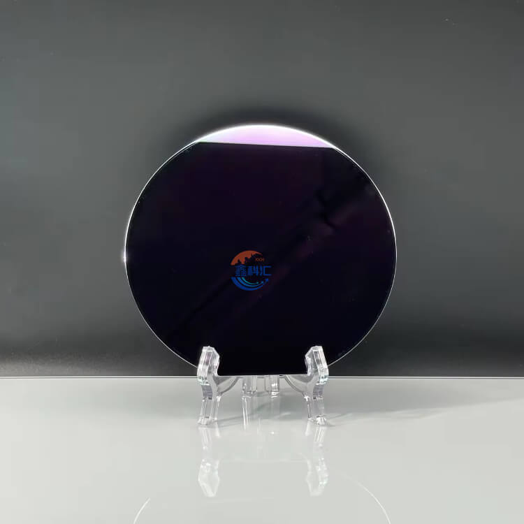
| Ytjämnhet. | < 0,5 nm |
| Anmärkningar. | Si-skiva med tillgängliga funktionella lager (termisk oxid SiO2, kiselnitrid Si3N4, etc.) |
Si wafers are a basic material used in semiconductor manufacturing and have many unique physical and chemical properties. Below is a detailed description of the properties of Si wafers and their importance in the semiconductor industry.
1. Kristallstruktur. The Si wafer is composed of pure silicon crystals, and its lattice structure belongs to the diamond cubic structure. Silicon atoms are joined together in covalent bonds to form a uniform crystal structure.
2. Kristallorientering. Si wafer usually has < 100> , < 110> < 111> Crystal orientation, which determines its specific use and performance in the manufacturing process.
3. Kristallyta. The surface of a Si wafer is usually a (100) or (111) crystal face, which has an important impact on different types of processing.
4. Storlek. Si wafer are typically 2, 4, 6, 8, or 12 inches in diameter, depending on the requirements of the final product and the limitations of the manufacturing process.
5. Tjocklek. Tjockleken på kiselskivor varierar typiskt mellan några hundra mikrometer till flera millimeter, beroende på tillverkningsprocessen och Tjockleken på kiselskivor varierar vanligtvis mellan några hundra mikrometer till flera millimeter, beroende på tillverkningsprocessen och.
6.Impurity content: Hög renhet är en av de viktigaste egenskaperna hos Si-wafers Renhetsnivåerna måste hållas extremt låga, vanligtvis mätt i miljondelar (ppm).
7. Elektronisk struktur. En kiselskiva är ett halvledarmaterial vars elektroniska struktur gör att den kan bli en ledare eller isolator när den är rätt dopad. Den elektriska elektriska ledningsförmågan hos en kiselskiva beror på typ och koncentration av dopning.
8. Optiska egenskaper. Si wafers have different transmission and reflection properties for different wavelengths of light, which are critical in photolithography and other semiconductor processing.

9. Mekaniska egenskaper. The Si wafer has excellent mechanical stability and hardness, which enables it to maintain shape stability in various processing processes.
10. Termiska egenskaper. Si wafers has good thermal conductivity and thermal stability, which is essential for the heat dissipation and stable operation of integrated circuits.
11. Kemisk reaktivitet. Si wafers have high chemical inertness to many chemicals, but they also react with some compounds under certain conditions, which requires attention during the manufacturing process.
12. Ytbehandling. Ytan på Si-skivor utsätts vanligtvis för en mängd olika behandlingar, såsom kemisk mekanisk polering (CMP), rengöring och beläggning, för att säkerställa ytans planhet och renhet. ytans planhet och renhet.
13. Gitterdefekter. Si wafers may have lattice defects, such as dislocations and grain boundaries, that can affect the electrical and mechanical properties of the wafer.
14. Elektronisk rörlighet. The electronic mobility of Si wafers is an important parameter when it is used in electronic devices such as transistors, which directly affects the speed and performance of the devices.
15. Fotoluminescens. In some special applications, Si wafers may exhibit photoluminescence properties, which have important implications in optoelectronics and sensor technology.
16. Kristalliseringsmetod. Kiselskivor kan framställas med en mängd olika metoder, t.ex. stelning, ångdeposition och diffusion i vätskefas, som var och en påverkar prestanda och kostnad för kiselskivor.
In general, Si wafers, as the fundamental material of the semiconductor industry, have a special set of physical, chemical and electronic properties that are critical to the manufacture and performance of modern electronic devices. Through continuous improvement of manufacturing processes and material properties, the performance and application range of silicon wafers continue to expand, driving the development and innovation of semiconductor technology.
Si wafers, with their unique properties and versatile characteristics, find widespread application across various industries and technological domains. From electronics to solar energy, Si wafers play a pivotal role in enabling innovation and advancement.
1. Semiconductor Industry: Silicon wafers serve as the fundamental substrate for manufacturing semiconductor devices, including microprocessors, memory chips, and integrated circuits (ICs). The semiconductor industry heavily relies on silicon wafers due to their excellent electrical properties and compatibility with semiconductor fabrication processes.
2. Integrated Circuits (ICs): Silicon wafers are the building blocks of integrated circuits, which are essential components in electronic devices such as smartphones, computers, and consumer electronics. The precise patterning and doping of silicon wafers enable the creation of complex electronic circuits on a microscopic scale.
3. Microelectronics: Si wafers are utilized in the production of various microelectronic components, including diodes, transistors, and sensors. These components form the backbone of modern electronic systems, facilitating functions such as signal processing, amplification, and sensing in diverse applications.
4. Photovoltaic (PV) Cells: Si wafers serve as the substrate for manufacturing photovoltaic cells, which convert sunlight into electricity. Photovoltaic technology is widely used in solar panels for residential, commercial, and industrial applications, contributing to renewable energy generation and sustainability efforts.
5. Solar Energy: Si wafers play a crucial role in the solar energy industry, where they are employed in both crystalline silicon and thin-film solar cell technologies. Silicon-based solar panels offer high efficiency, reliability, and scalability, making them a preferred choice for harnessing solar power in grid-connected and off-grid systems.
6. Optoelectronics: Si wafers are utilized in optoelectronic devices such as light-emitting diodes (LEDs), photodetectors, and optical fibers. These devices enable applications in telecommunications, display technologies, medical imaging, and industrial sensing, among others, by converting between electrical and optical signals.
7. MEMS (Microelectromechanical Systems): Silicon wafers serve as substrates for fabricating MEMS devices, which integrate mechanical and electrical components on a microscopic scale. MEMS technology enables the development of sensors, actuators, and microfluidic systems for applications in automotive, healthcare, aerospace, and consumer electronics.
8. Biomedical Devices: Silicon wafers are utilized in the production of biomedical devices and implants for diagnostic, therapeutic, and prosthetic applications. Silicon-based sensors, microfluidic devices, and neural interfaces play a crucial role in advancing healthcare technologies, including wearable devices, implantable sensors, and lab-on-a-chip systems.
9. Microfluidics: Silicon wafers are employed in microfluidic systems for precise manipulation and analysis of fluids on a miniaturized scale. Microfluidic devices find applications in chemical synthesis, biomedical diagnostics, drug discovery, and environmental monitoring, offering advantages such as reduced sample volumes, rapid analysis, and integration with other analytical techniques.
10. Wafer Bonding and Packaging: Silicon wafers undergo wafer bonding processes to integrate multiple layers or devices, enabling the fabrication of advanced semiconductor structures and heterogeneous systems. Wafer-level packaging techniques enhance the performance, reliability, and miniaturization of electronic and optoelectronic devices, supporting diverse applications in electronics, photonics, and MEMS.


In the realm of semiconductor manufacturing, Si wafers serve as the fundamental building blocks for integrated circuits (ICs) and microchips, which are integral components of virtually all electronic devices, including smartphones, computers, and automotive systems. The precise properties and high purity of silicon wafers are critical for ensuring the performance, reliability, and scalability of these semiconductor devices, which continue to evolve in complexity and functionality.
Moreover, Si wafers play a pivotal role in advancing renewable energy technologies such as solar photovoltaics (PV). Solar cells, which convert sunlight into electricity, rely on silicon wafers as the substrate for fabricating solar panels. The widespread adoption of silicon-based solar cells has contributed to the expansion of solar energy generation worldwide, driving progress towards a more sustainable and environmentally friendly energy landscape.
Beyond electronics and energy, Si wafers find applications in various healthcare technologies, including biomedical sensors, diagnostic devices, and medical implants. Silicon-based microelectronics enable the miniaturization, integration, and precision necessary for developing advanced medical devices that enhance diagnosis, treatment, and patient care.
Furthermore, Si wafers are integral to emerging technologies such as quantum computing, nanotechnology, and Internet of Things (IoT) devices, which are poised to revolutionize computing, communications, and data analytics. These cutting-edge applications leverage the unique properties of silicon and exploit the scalability and manufacturability of silicon wafers to enable novel functionalities and unprecedented capabilities.
As material science, processing techniques, and device integration continue to advance, Si wafers are expected to play an increasingly indispensable role in driving innovation and enabling transformative technologies in the digital age. Research and development efforts focused on enhancing the performance, efficiency, and functionality of silicon-based devices will further expand the range of applications for silicon wafers, unlocking new opportunities for technological advancement and economic growth.
In summary, Si wafers serve as versatile platforms that underpin a diverse array of applications across multiple industries, from semiconductor manufacturing and electronics to renewable energy, healthcare, and beyond. Their crucial role in enabling technological innovation and progress underscores the enduring significance of silicon wafers in shaping the modern world and driving forward the digital revolution.
The choice of Si wafers depends on the application. Single crystal wafers are the most common choice for ICs, while polycrystalline wafers are often used for solar cells and LEDs. Amorphous silicon wafers are less common, but they are sometimes used for applications where cost is a major consideration.
A Si wafer is made by spinning molten silicon in a crucible. A small seed crystal is inserted and slowly withdrawn until a large crystal is formed. Upon completion, a large, solid silicon wafer weighing several hundred pounds is produced. The chip is then tested to ensure its purity.
Si wafers technology is crucial for achieving high-quality IC packaging performance. Thin silicon wafers offer better thermal conductivity, minimize warpage, and support miniaturization – ideal for advanced IC packaging for compact electronic devices.
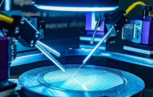
This testing process requires the application of a piece of equipment called a wafer prober. Wafer probing machines are automatic testing equipment used in the semiconductor manufacturing process to electrically test the integrated circuits of each wafer die.