
Silicon wafers have several advantages, especially in the semiconductor industry:
1. Semiconductor Fabrication: Silicon wafers are the foundational material for manufacturing integrated circuits (ICs) and other semiconductor devices. Their high purity and crystalline structure make them ideal for this purpose.
2. Electrical Properties: Silicon has excellent electrical properties, such as high carrier mobility and a stable oxide layer (silicon dioxide), which is essential for creating reliable semiconductor devices.
3. Uniformity: Silicon wafers can be manufactured with high uniformity in terms of thickness, resistivity, and crystal orientation, ensuring consistent performance across a batch of semiconductor devices.
4. Compatibility: Silicon wafers are compatible with a wide range of semiconductor processing techniques, including doping, etching, and deposition methods, making them versatile for various device fabrication processes.
5. Scaling: Silicon wafers have allowed for the scaling down of transistor sizes, enabling the continuous improvement of semiconductor devices’ performance and density (Moore’s Law).
6. Mechanical Properties: Silicon wafers are mechanically robust and can withstand the stresses associated with semiconductor processing steps like polishing, etching, and lithography.
7. Cost Efficiency: Despite being a high-tech material, silicon wafers benefit from economies of scale due to widespread use in the semiconductor industry, which helps in keeping production costs relatively low compared to other materials.
These advantages collectively contribute to silicon wafers being the material of choice for manufacturing modern semiconductor devices used in electronics, computing, and telecommunications.
Кремниевые пластины (Si wafers) - основной материал, используемый в производстве полупроводников и обладающий множеством уникальных физических и химических свойств. Ниже приводится подробное описание свойств Si wafers и их важности в полупроводниковой промышленности. Подробное описание свойств Si пластин и их важности в полупроводниковой промышленности.
1. Кристаллическая структура. The silicon wafer is composed of pure silicon crystals, and its lattice structure belongs to the diamond cubic structure. Silicon atoms are joined together in covalent bonds to form a uniform crystal structure.
2. Ориентация кристаллов. Silicon wafer usually has < 100> , < 110> < 111> Crystal orientation, which determines its specific use and performance in the manufacturing process.
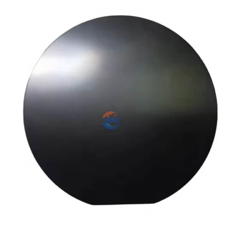
3. Хрустальный лик. The surface of a silicon wafer is usually a (100) or (111) crystal face, which has an important impact on different types of processing.
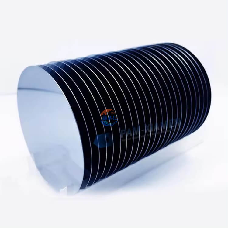
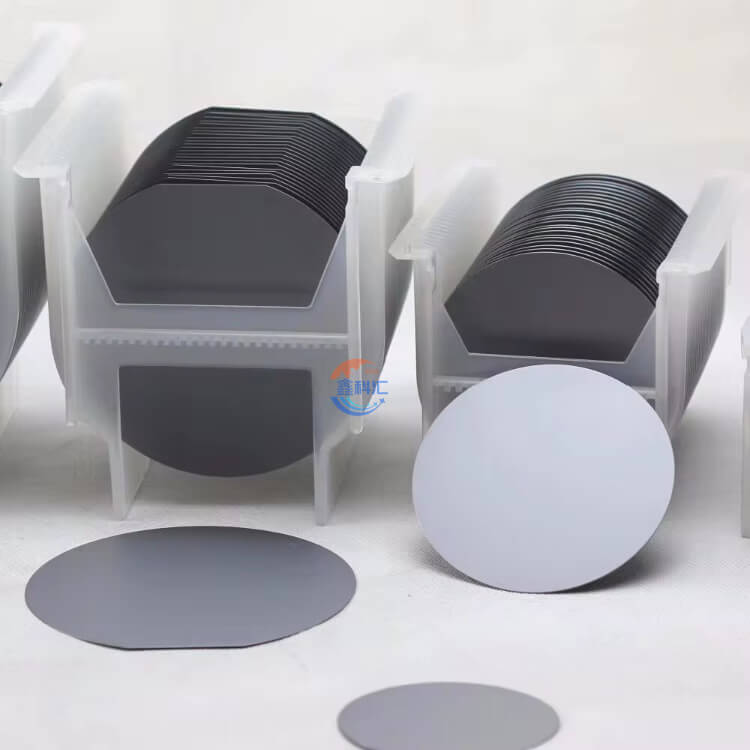
4. Размер. Silicon wafers are typically 2, 4, 6, 8, or 12 inches in diameter, depending on the requirements of the final product and the limitations of the manufacturing process.
5. Толщина. Толщина кремниевых пластин обычно варьируется от нескольких сотен микрон до нескольких миллиметров, в зависимости от процесса производства и Толщина кремниевых пластин обычно варьируется от нескольких сотен микрон до нескольких миллиметров, в зависимости от производственного процесса и.
6. Impurity content: Высокая чистота - одна из ключевых характеристик Si пластин Уровень примесей должен быть крайне низким, обычно измеряется в частях на миллион (ppm).
7. Электронная структура. Кремниевая пластина - это полупроводниковый материал, электронная структура которого позволяет ему становиться проводником или изолятором при соответствующем легировании. Электрическая электропроводность кремниевой пластины зависит от типа и концентрации легирования.
8. Оптические свойства. Silicon wafers have different transmission and reflection properties for different wavelengths of light, which are critical in photolithography and other semiconductor processing.
9. Механические свойства. The silicon wafer has excellent mechanical stability and hardness, which enables it to maintain shape stability in various processing processes.
10. Тепловые характеристики. Silicon has good thermal conductivity and thermal stability, which is essential for the heat dissipation and stable operation of integrated circuits.
11. Химическая реактивность. Silicon wafers have high chemical inertness to many chemicals, but they also react with some compounds under certain conditions, which requires attention during the manufacturing process.
12. обработка поверхности. Поверхность Si пластин обычно подвергается различным видам обработки, таким как химико-механическая полировка (CMP), очистка и нанесение покрытия, для обеспечения плоскостности и чистоты поверхности. ровность и чистоту поверхности.
13. Дефекты решетки. Silicon wafers may have lattice defects, such as dislocations and grain boundaries, that can affect the electrical and mechanical properties of the wafer.
14. Электронная мобильность. The electronic mobility of silicon wafers is an important parameter when it is used in electronic devices such as transistors, which directly affects the speed and performance of the devices.
15. Фотолюминесценция. In some special applications, silicon wafers may exhibit photoluminescence properties, which have important implications in optoelectronics and sensor technology.
16. Метод кристаллизации. Силиконовые пластины могут быть получены различными методами, такими как затвердевание, осаждение из паровой фазы и жидкофазная диффузия, каждый из которых влияет на производительность и стоимость кремниевых пластин.
| Продукт. | Кремниевая (Si) пластина |
| Оценка. | IC prime grade |
| Чистота. | >99.99999999999% (11N) |
| Размеры. | Стандартные размеры.- 1” × 0,5 мм- 2” × 0,28 / 0,4 / 0,5 мм- 3” × 0,38 мм- 4” × 0,525 мм- 5” × 0,6 мм- 6” × 0,625 мм- 8” × 0,725 мм " × 0,525 мм- 5" × 0,6 мм- 6" × 0,625 мм- 8" × 0,725 мм Возможны другие диаметры и толщины- Мы предоставляем небольшие нестандартные пластины для исследовательских/испытательных целей. |
| Ориентация. | / / / вне оси / другие |
| Проводящий тип. | - Нелегированный (также называемый внутренним, собственным) тип- N-тип: легированный люминофором (P)- P-тип: легированный бором (B) |
| Сопротивление. | Стандартное удельное сопротивление для недопированных пластин.- 3000 - 6000 Ω-см Стандартное удельное сопротивление для подложек n-/ p-типа.- 0,001 - 0,009 Ω-см - 1 - 10 Ω-см - 10 - 20 Ω-см - 90 - 100 Ω-см Доступны другие удельные сопротивления |
| Полировка. | - Пластины без полировки - Односторонняя эпиполировка - Двухсторонняя эпиполировка |
| Шероховатость поверхности. | < 0,5 нм |
| Примечания. | Si пластина с имеющимися функциональными слоями (термооксид SiO2, нитрид кремния Si3N4 и т.д.) |